



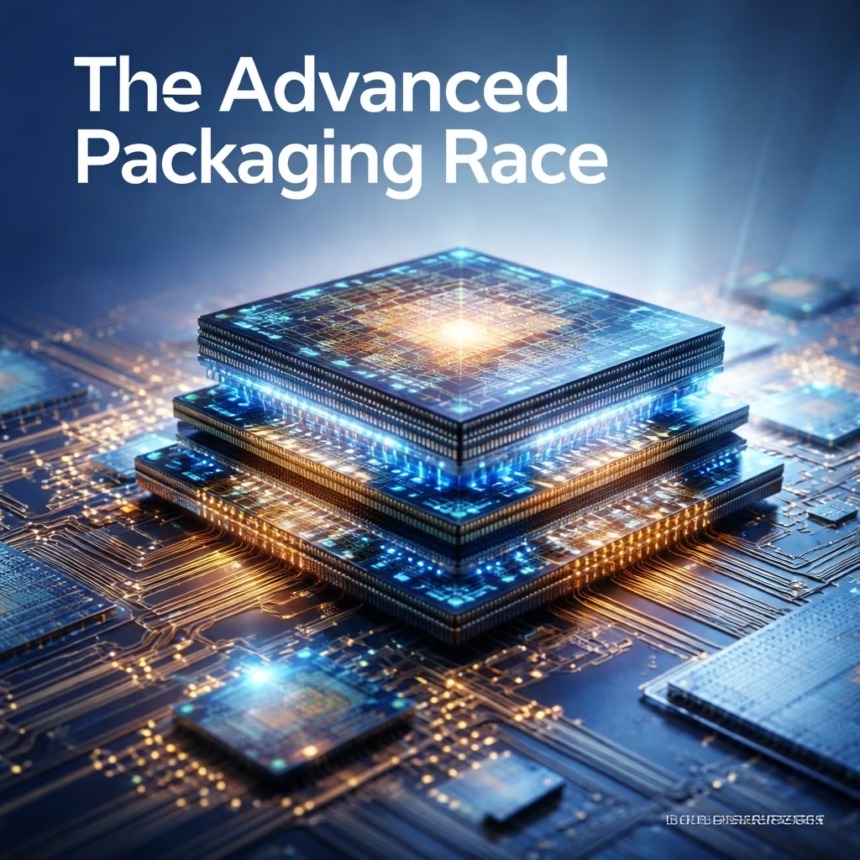
A fierce, multi-billion dollar competition is escalating across the global semiconductor industry, centered on advanced chip packaging technologies. This crucial race, unfolding primarily in East Asia and increasingly in the West, is dictating the future performance and power efficiency of AI accelerators, high-performance computing (HPC), and data center infrastructure as early as 2024. As traditional chip scaling encounters physical limits, the ability to intricately stack and connect components has become the new frontier in the quest for computational dominance.
Background: The New Frontier Beyond Moore’s Law
For decades, Moore's Law drove semiconductor innovation, predicting a doubling of transistors on an integrated circuit every two years. However, shrinking transistors to single-digit nanometer scales has become exponentially complex and expensive. This physical bottleneck has propelled advanced packaging from a supporting role to a central pillar of chip design and manufacturing.
The End of Scaling: Why Packaging Matters
Advanced packaging techniques enable chipmakers to overcome the limitations of monolithic designs. Instead of fabricating an entire complex system on a single, massive piece of silicon, these methods allow for the integration of multiple smaller "chiplets" or memory stacks into a single, high-performance package. This modular approach improves yield, reduces costs for specialized functions, and enhances performance by minimizing signal latency and power consumption.
Early Innovators: HBM and 2.5D
The journey into advanced packaging gained significant traction in the early 2010s. High Bandwidth Memory (HBM), pioneered by SK Hynix and Samsung, emerged around 2013, stacking multiple DRAM dies vertically with through-silicon vias (TSVs) to achieve unprecedented memory bandwidth. This innovation led to 2.5D packaging, where a silicon interposer acts as a bridge, connecting a processor die and HBM stacks side-by-side within a single package. AMD's Fiji GPU in 2015 was an early adopter, showcasing the potential for graphics and high-performance computing.
Foundries like TSMC, Intel, and Samsung quickly developed their proprietary 2.5D and early 3D solutions. TSMC's CoWoS (Chip-on-Wafer-on-Substrate), Intel's EMIB (Embedded Multi-die Interconnect Bridge), and Samsung's I-Cube were foundational technologies, laying the groundwork for the current packaging arms race.
More Read

Key Developments: AI’s Insatiable Demand Ignites the Race
The explosion of generative AI and large language models has dramatically accelerated the demand for advanced packaging, particularly for high-end AI accelerators. NVIDIA's H100 GPU, for instance, relies heavily on TSMC's CoWoS technology to integrate its powerful GPU die with six stacks of HBM3 memory.
AI’s Insatiable Demand
The unprecedented computational requirements of AI training and inference have pushed HBM and advanced packaging capacity to their limits. In late 2023 and early 2024, reports indicated a significant bottleneck in CoWoS capacity at TSMC, directly impacting the supply of NVIDIA's leading AI GPUs. This shortage has spurred massive investment and expansion plans across the industry.

Foundry Giants Lead the Charge
TSMC, the dominant player in logic foundry services, continues to expand its CoWoS capacity aggressively. The Taiwanese giant plans to double its CoWoS output by 2025, with new facilities in Taiwan and potentially Japan. Its SoIC (System-on-Integrated-Chips) platform, offering true 3D stacking with hybrid bonding, represents the next generation of integration, enabling even denser and more power-efficient designs.
Intel is heavily investing in its Foveros and Foveros Direct technologies, aiming for leadership in hybrid bonding and 3D stacking. Its IDM 2.0 strategy includes significant packaging capacity expansion at its Arizona and New Mexico sites, supported by the U.S. CHIPS Act. Products like the Meteor Lake client processor and upcoming Xeon processors utilize these advanced packaging techniques.
Samsung Foundry is also a formidable contender with its I-Cube (2.5D) and X-Cube (3D) platforms. The South Korean conglomerate is aggressively ramping up HBM production and advanced packaging services to secure a larger share of the AI chip market, particularly through its turnkey solutions that encompass memory, logic, and packaging.
OSATs Step Up
Outsourced Semiconductor Assembly and Test (OSAT) companies play a critical role in this ecosystem. Giants like Amkor Technology, ASE Technology Holding (including ASE and SPIL), and JCET Group are investing billions to expand their advanced packaging capabilities. Amkor, for instance, opened a new advanced packaging facility in Peoria, Arizona, in 2024, partly to support U.S. domestic semiconductor manufacturing initiatives. These OSATs are crucial for providing diversified capacity and specialized solutions beyond what the integrated device manufacturers (IDMs) and pure-play foundries offer.
New Technologies and Materials
Beyond 2.5D and early 3D stacking, hybrid bonding is emerging as a critical enabler for true die-to-die and wafer-to-wafer stacking with ultra-fine pitch interconnects. This technology, which directly bonds chip layers using copper-to-copper connections, significantly reduces interconnect length, enhancing performance and power efficiency. Innovations in substrate materials, thermal management solutions, and advanced testing equipment are also rapidly evolving to support these complex architectures.
Impact: Reshaping Industries and Geopolitics
The advanced packaging race has profound implications for various industries, supply chains, and global power dynamics.
More Read

AI Accelerators and Data Centers
The most immediate and significant impact is on the AI and HPC sectors. Companies like NVIDIA, AMD, Broadcom, and major hyperscalers (Google, Amazon, Microsoft) are critically dependent on advanced packaging to build their next-generation AI accelerators and data center CPUs. Without these technologies, the performance gains necessary to drive AI innovation would be severely hampered. The ability to integrate HBM3E and future HBM4 memory with powerful processors in a compact, efficient package is paramount.
Consumer Electronics and Edge AI
While AI accelerators are the primary driver, advanced packaging also enables smaller, more powerful, and energy-efficient chips for consumer electronics, automotive applications, and edge AI devices. Miniaturization and performance gains allow for more sophisticated AI capabilities directly on devices, reducing reliance on cloud processing.
Supply Chain Complexity and Resilience
The reliance on a few key players and specific regions for advanced packaging creates supply chain vulnerabilities. The concentration of cutting-edge packaging capacity in Taiwan, particularly at TSMC, has become a geopolitical concern. This has spurred efforts in the U.S., Europe, and Japan to diversify and localize advanced packaging capabilities, aiming to build more resilient semiconductor ecosystems.
Geopolitical Stakes
Governments worldwide recognize advanced packaging as a strategic technology. The U.S. CHIPS and Science Act, the European Chips Act, and Japan's initiatives (like the Rapidus consortium) include substantial funding for advanced packaging research, development, and manufacturing. This is driven by economic competitiveness, national security, and the desire to control critical aspects of the future technology landscape.
What Next: The Road Ahead for Integration
The advanced packaging race is far from over, with several critical milestones and challenges on the horizon.
Capacity Expansion and Diversification
The immediate future will see continued, aggressive expansion of advanced packaging capacity. TSMC, Intel, and Samsung are projected to significantly increase their output of CoWoS, Foveros, and I-Cube/X-Cube solutions through 2025 and 2026. This expansion will likely involve a more geographically diverse footprint, with new fabs and assembly sites emerging in the U.S., Japan, and potentially Europe, driven by government incentives and strategic imperatives.
The Evolution of HBM and 3D Stacking
The next generation of HBM, HBM4, is already in development, promising even higher bandwidth and capacity. Its integration will push the boundaries of 3D stacking, potentially leveraging hybrid bonding for direct chip-to-chip connections between logic and memory layers. This will enable even more compact and power-efficient designs, crucial for exascale computing and future AI models.
Hybrid Bonding Maturity and Standardization
Hybrid bonding is expected to become more mainstream for high-volume manufacturing, moving beyond niche applications. As more components are integrated using this technology, challenges related to yield, thermal management, and testing will need to be overcome. Furthermore, industry-wide standardization efforts, such as the UCIe (Universal Chiplet Interconnect Express) consortium, will be vital to ensure interoperability between chiplets from different vendors, fostering a more open and competitive chiplet ecosystem.
New Materials, Equipment, and Testing
Innovation in materials science will be critical, especially for thermal interface materials and advanced substrates that can dissipate heat from densely packed 3D structures. The development of new inspection, metrology, and test equipment capable of handling the extreme complexity of advanced packages will also be paramount. Testing 3D stacked chips presents unique challenges that require novel approaches.
Addressing the Challenges
Despite the rapid advancements, significant hurdles remain. The escalating costs of advanced packaging, the complexity of design and manufacturing, yield management, and the thermal challenges of packing more power into smaller volumes are constant concerns. The industry will need collaborative efforts across the supply chain, from material suppliers to equipment manufacturers, foundries, and OSATs, to navigate these complexities and ensure the continued progress of semiconductor technology.